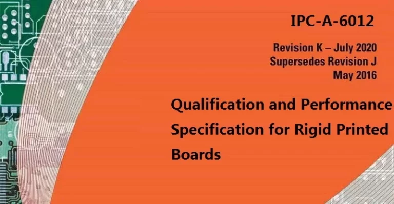
IPC Class 2 & Class 3 PCB Manufacturing: Requirements, DFM & Verification
Engineering guide to IPC Class 2 and Class 3 rigid PCB manufacturing, including DFM, plated holes, annular ring, inspection, verification, and procurement requirements.

Engineering guide to IPC Class 2 and Class 3 rigid PCB manufacturing, including DFM, plated holes, annular ring, inspection, verification, and procurement requirements.
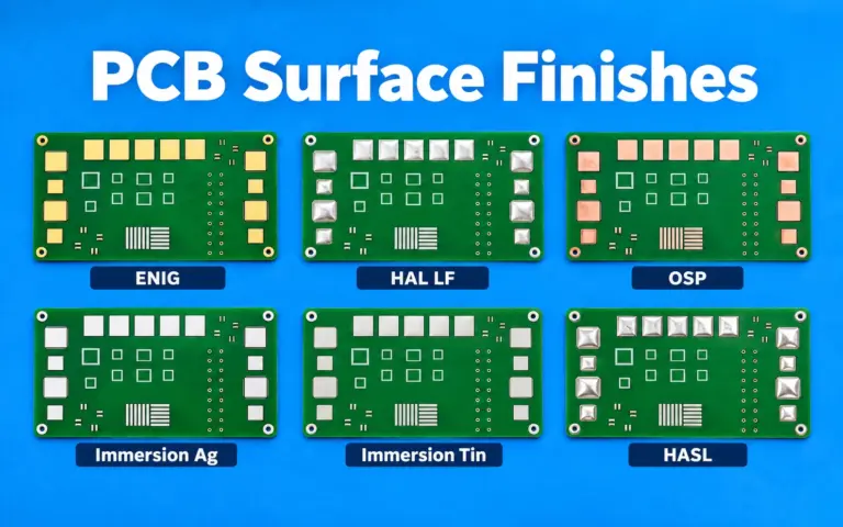
PCB surface finishes protect exposed copper pads and help ensure reliable soldering performance in electronic assemblies. Printed Circuit Boards (PCBs) are used in a wide range of products, including consumer
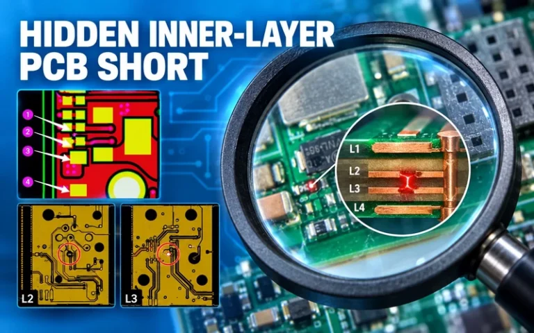
A WellerPCB manufacturing case study on why correct working Gerber data does not always guarantee a defect-free multilayer PCB The central lesson is clear: if a PCB-based product is intended
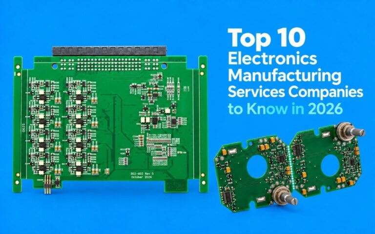
Electronics manufacturing services companies differ significantly in scale, technical specialization, service scope, and the types of programs they are built to support. Foxconn and Wistron operate at enormous global scale,

Electronic Manufacturing Services (EMS) is an outsourcing model in which a specialist manufacturer builds electronic assemblies or finished products for an OEM or product company under an agreed specification. Depending
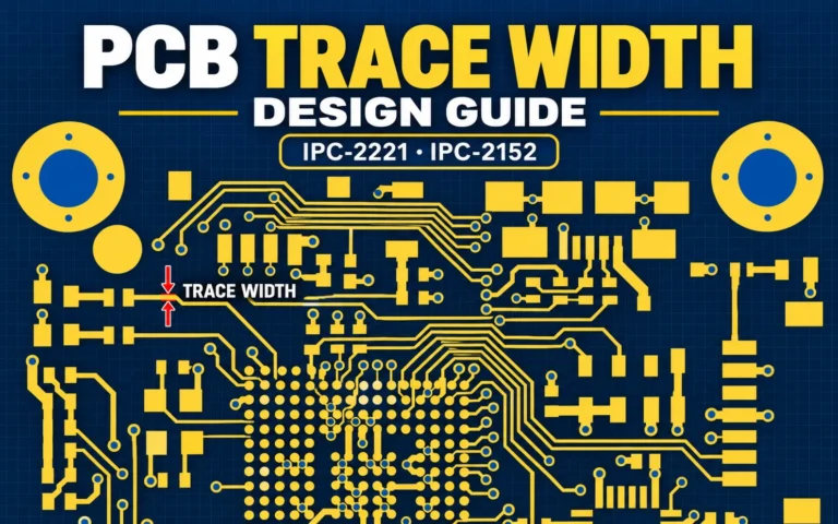
Introduction PCB trace is the copper trace on the PCB board that connects different electronic components. A trace that is too narrow for the current it carries can generate excessive
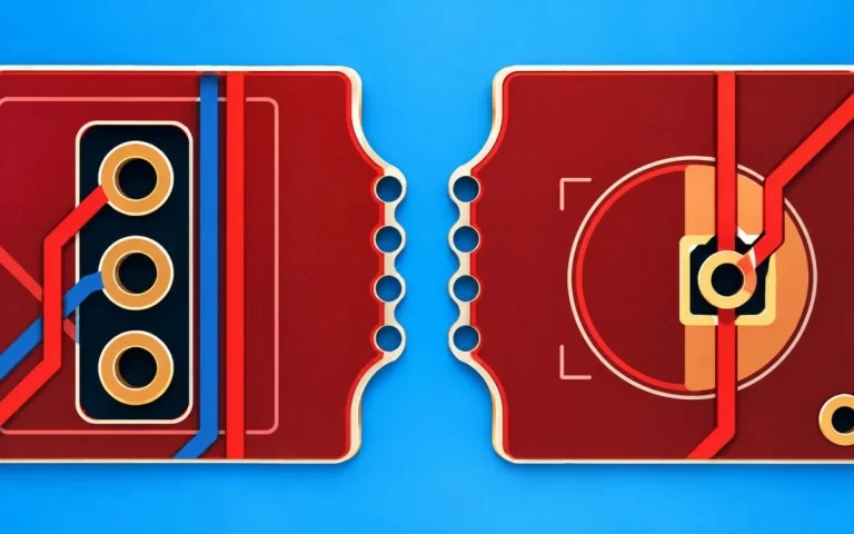
PCB mouse bites are perforated breakaway tabs that hold boards in a routed panel and allow controlled separation after assembly. Their performance depends on hole geometry, tab placement, board thickness,
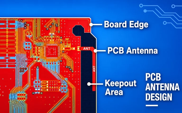
PCB antenna design depends on more than the radiator shape. The antenna, ground plane, feed line, matching network, PCB stackup, enclosure, battery, and nearby metal operate as one RF structure.
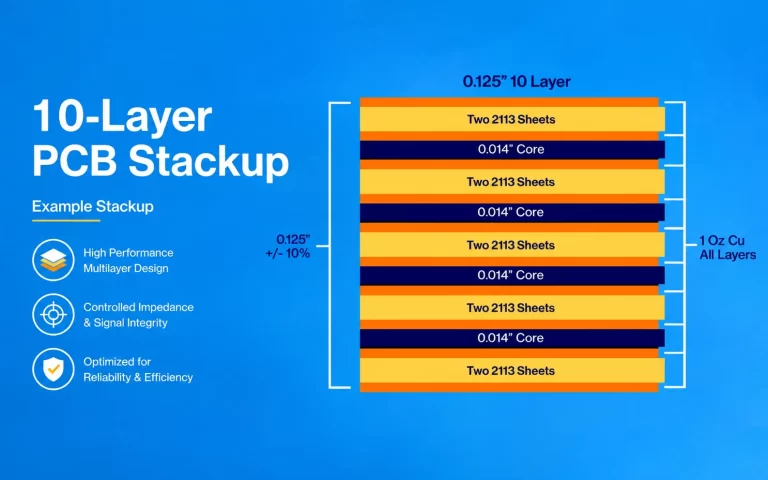
Your PCB stackup, both literally and figuratively, is the foundation for your new product. Although the PCB stackup enables everything in your layout, it imposes important constraints on routing and
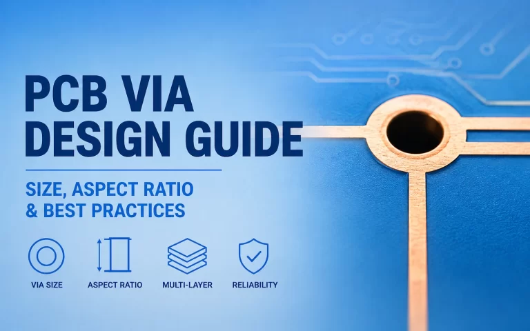
Introduction A via may look like a simple hole in a PCB, but its drill diameter, pad diameter, annular ring, board thickness, plating, and layer transition all affect whether it
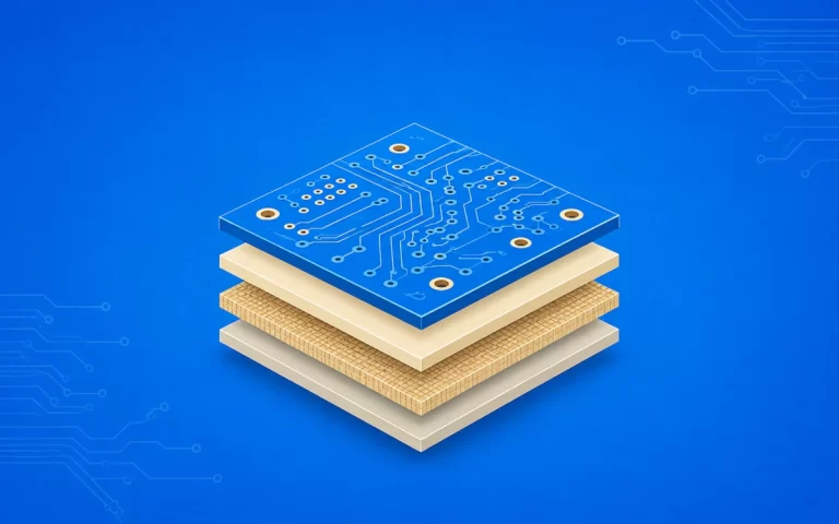
In PCB design and manufacturing, engineers usually focus on impedance control, thermal performance, stackup structure, and signal integrity. However, the base material itself determines another critical reliability factor: Comparative Tracking
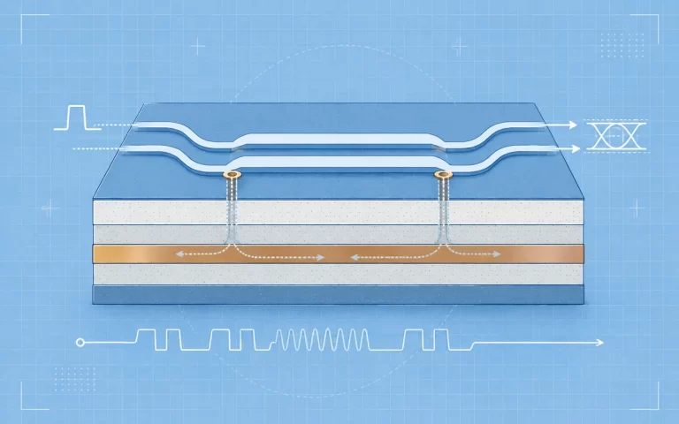
High-speed PCB design becomes necessary when the PCB interconnect starts to affect the voltage or timing seen by the receiver. There is no single clock-frequency threshold that tells you when